
Can New 3D Chips Revolutionize Electronics with Speed and Efficiency?
Revolutionizing Electronics: The Future of Gallium Nitride Integration with Silicon
In the world of electronic devices and communication systems, the importance of high-performance semiconductors cannot be overstated. Among these, gallium nitride (GaN) stands out due to its exceptional properties that make it suitable for high-speed communication and power electronics. However, despite its potential, the high cost and complexity of integrating GaN into conventional electronics have hindered its widespread adoption. Recent advancements from researchers at MIT and other institutions have paved the way for a breakthrough fabrication process that integrates GaN transistors onto standard silicon chips in a cost-effective and scalable manner. This article will delve into the significance of this development, the technology behind it, and its implications for the future of electronic devices.
The Promise of Gallium Nitride
Gallium nitride is the second most widely used semiconductor globally, following silicon. Its unique properties, including high electron mobility, wide bandgap, and thermal stability, make it an ideal material for various applications, including:
- High-frequency RF (Radio Frequency) devices
- Power amplifiers in telecommunications
- LED lighting and displays
- Radar systems
- Power electronics for electric vehicles
Despite its advantages, the integration of GaN into existing silicon-based technologies has been a challenge due to the specialized fabrication techniques required and the associated costs. Traditional methods of bonding GaN to silicon often involve expensive materials like gold and high-temperature processes that can damage the delicate structures of both types of chips. This has limited the commercial viability of GaN applications in everyday electronics.
Innovative Fabrication Process
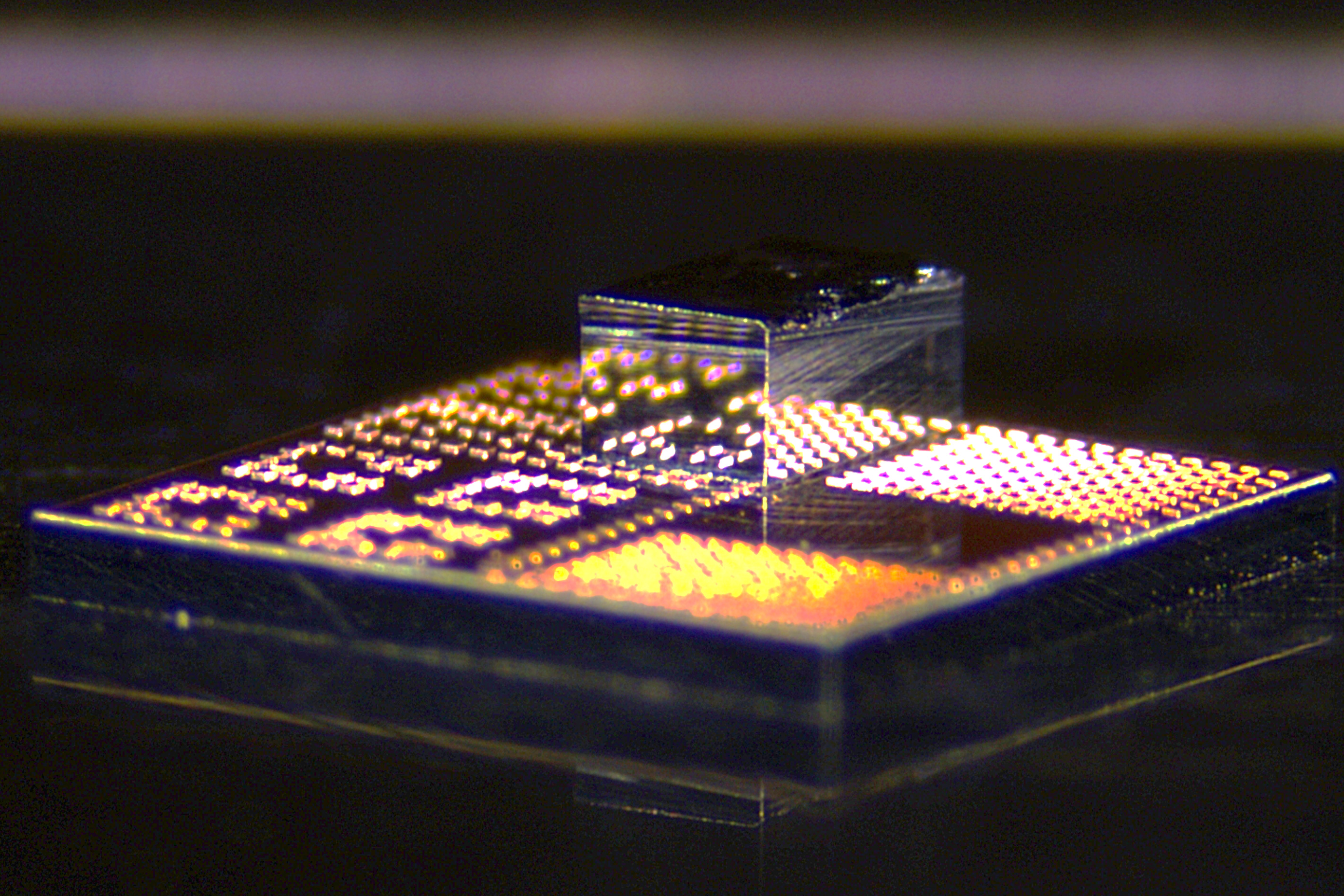
Researchers at MIT have developed a novel approach to overcome these challenges, allowing for the efficient integration of GaN transistors onto standard silicon CMOS chips. The key innovation is a multi-step fabrication process that incorporates tiny GaN transistors, known as dielets, onto silicon without the need for costly materials or high temperatures.
Step-by-Step Breakdown of the Fabrication Process
- Wafer Preparation: The process begins with the fabrication of densely packed GaN transistors across the entire surface of a GaN wafer. Each transistor is meticulously designed to maximize performance, measuring just 240 by 410 microns.
- Dielet Cutting: Using precision laser technology, individual transistors are cut from the wafer, creating small, manageable dielets that can be easily handled.
- Copper Bonding: Each dielet is equipped with tiny copper pillars, which are used to create a bond with corresponding pillars on the silicon CMOS chip. This bonding is performed at low temperatures (below 400 degrees Celsius), preventing damage to either material.
- Integration Tool: A specialized tool utilizing vacuum technology holds the dielet in place, allowing for precise positioning over the silicon chip. Once aligned, heat and pressure are applied to form a solid bond.
This innovative method not only reduces the amount of GaN material required but also enhances the performance of the resulting devices. By distributing the GaN transistors across the silicon chip, researchers can effectively manage heat dissipation, which is crucial for maintaining optimal performance in electronic systems.
Applications and Benefits of GaN-Silicon Hybrid Chips
The implications of this new fabrication process are vast, particularly in the realm of mobile communication and data centers. A notable demonstration conducted by the researchers involved the development of a power amplifier, a critical component in mobile phones. The results showed that the GaN-based power amplifier achieved:
- Higher Signal Strength: Compared to traditional silicon transistors, the GaN amplifiers demonstrated significantly improved signal strength, which can enhance call quality and data transmission.
- Increased Efficiency: The efficiency of these devices allows for better power usage, extending battery life in smartphones and other portable devices.
- Enhanced Connectivity: With improved bandwidth capabilities, users can expect faster and more reliable connections, which are vital as data consumption continues to rise.
Potential for Future Technologies
Beyond immediate applications, the hybrid chips could also play a pivotal role in the advancement of future technologies. The compatibility of GaN with silicon opens doors to innovations in:
- Quantum Computing: GaN's superior performance at cryogenic temperatures positions it as a strong candidate for quantum applications, which are becoming increasingly significant in computing.
- AI and Machine Learning: The integration of GaN transistors could lead to enhanced processing capabilities, beneficial for AI algorithms that require rapid data analysis.
- Next-Generation Wireless Technologies: As 5G networks and beyond continue to evolve, the need for efficient and powerful RF components will grow. GaN's properties make it ideal for these next-gen communication systems.
Challenges and Considerations
While the new fabrication process presents a significant leap forward in semiconductor technology, several considerations must be addressed for widespread adoption:
- Commercialization: The transition from research to practical, scalable manufacturing processes is crucial. Collaborations with semiconductor foundries will be essential to integrate this technology into existing manufacturing lines.
- Cost Management: Although the new method reduces costs associated with GaN integration, ongoing efforts are needed to ensure that production remains economically viable for commercial applications.
- Market Acceptance: Educating industries about the benefits of GaN technology and addressing any concerns regarding reliability and performance will be key to fostering adoption.
Conclusion: A New Era for Semiconductor Technology
The advances in integrating gallium nitride with silicon represent a pivotal moment in semiconductor technology. By effectively combining the strengths of both materials, researchers have created a pathway that enhances performance while reducing costs. This innovation could lead to a new era in electronics where high-speed communication and efficient power management become the norm.
As we stand on the brink of this technological revolution, it is clear that the potential of gallium nitride is just beginning to be realized. The implications are not only exciting for the immediate future of consumer electronics but also for the broader landscape of technology that underpins our digital lives. Manufacturers and consumers alike must stay informed and engaged with these developments, as they promise to redefine our relationship with technology.
FAQs about Gallium Nitride Integration with Silicon
What is gallium nitride and why is it important?
Gallium nitride (GaN) is a semiconductor material known for its high efficiency, high power density, and capability to operate at high temperatures. Its unique properties make it ideal for applications in power electronics, RF devices, and next-generation communication systems.
How does the new fabrication process work?
The new fabrication process involves creating tiny GaN transistors, cutting them into dielets, and bonding them to silicon chips using copper pillars. This method is cost-effective, low-temperature, and scalable, making it compatible with existing semiconductor manufacturing processes.
What are the benefits of integrating GaN with silicon?
Integrating GaN with silicon allows for enhanced performance in electronic devices, including higher signal strength, improved efficiency, and greater bandwidth. This hybrid approach can lead to better battery life in smartphones and more reliable connectivity.
As technology continues to evolve, how do you see the integration of materials like gallium nitride reshaping the electronics landscape? #GalliumNitride #SemiconductorRevolution #TechInnovation
Published: 2025-06-18 04:00:00 | Category: Uncategorized